How Stacked CMOS Image Sensors Are Redefining Camera Technology: Unveiling the Breakthroughs Powering Next-Gen Imaging Performance
- Introduction: What Are Stacked CMOS Image Sensors?
- How Stacked Architecture Differs from Traditional CMOS Sensors
- Key Advantages: Speed, Quality, and Miniaturization
- Breakthrough Applications in Smartphones and Beyond
- Technical Innovations: Layered Design and Signal Processing
- Challenges and Limitations Facing Stacked CMOS Sensors
- Market Impact and Leading Manufacturers
- Future Trends: AI Integration and Next-Gen Imaging
- Conclusion: The Road Ahead for Stacked CMOS Image Sensors
- Sources & References
Introduction: What Are Stacked CMOS Image Sensors?
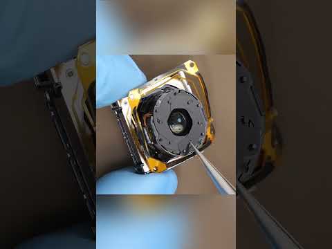
Stacked CMOS image sensors represent a significant advancement in digital imaging technology, offering improved performance and new functionalities compared to traditional CMOS sensors. In a conventional CMOS image sensor, all components—including the photodiodes (which capture light) and the circuitry for signal processing—are fabricated on a single silicon substrate. In contrast, stacked CMOS image sensors separate these functions into multiple layers, or “stacks,” which are then bonded together. Typically, the top layer contains the pixel array, while the bottom layer houses the signal processing circuitry. This architecture enables each layer to be optimized independently, leading to enhanced image quality, faster readout speeds, and reduced noise.
The stacking process is made possible by advanced semiconductor manufacturing techniques, such as through-silicon vias (TSVs), which allow electrical connections to pass vertically between layers. This separation of functions not only allows for more complex and efficient circuit designs but also frees up valuable space on the sensor surface, enabling the integration of additional features such as on-chip memory or advanced autofocus systems. As a result, stacked CMOS image sensors are particularly well-suited for applications demanding high performance in compact form factors, such as smartphones, digital cameras, and automotive imaging systems.
The adoption of stacked CMOS image sensors has accelerated in recent years, driven by the demand for higher resolution, better low-light performance, and advanced computational photography features. Leading manufacturers, including Sony Semiconductor Solutions and Samsung Semiconductor, have played a pivotal role in commercializing this technology, making it a cornerstone of modern digital imaging.
How Stacked Architecture Differs from Traditional CMOS Sensors
Stacked CMOS image sensors represent a significant evolution from traditional CMOS sensor architectures, primarily through their innovative use of vertically integrated layers. In conventional CMOS sensors, all pixel and circuit components—such as photodiodes, analog-to-digital converters, and signal processing circuits—are fabricated on a single silicon substrate. This monolithic approach imposes limitations on pixel size reduction, circuit complexity, and overall sensor performance due to the constraints of a single-layer design.
In contrast, stacked CMOS image sensors separate the pixel array and the logic circuitry into distinct layers, which are then bonded together using advanced wafer stacking techniques. The top layer typically contains the photodiodes and color filters, optimized for light absorption and image capture, while the bottom layer houses the signal processing and control circuits. This separation allows each layer to be manufactured using process technologies best suited to their specific functions, enabling smaller pixels, higher resolution, and more sophisticated on-chip processing without increasing the sensor’s footprint.
The stacked architecture also facilitates the integration of additional features, such as high-speed memory or artificial intelligence processing units, directly beneath the pixel layer. This not only enhances performance but also reduces power consumption and improves data throughput. As a result, stacked CMOS sensors deliver superior image quality, faster readout speeds, and greater flexibility for advanced imaging applications compared to their traditional counterparts. For further technical details, see Sony Semiconductor Solutions Corporation and Canon Inc..
Key Advantages: Speed, Quality, and Miniaturization
Stacked CMOS image sensors offer significant advancements over traditional front- and back-illuminated designs, particularly in the areas of speed, image quality, and device miniaturization. By separating the pixel layer from the logic circuitry and stacking them vertically, manufacturers can optimize each layer independently, leading to substantial performance gains.
One of the primary advantages is increased readout speed. The stacked architecture allows for dedicated signal processing circuits directly beneath the pixel array, enabling faster data transfer and parallel processing. This results in higher frame rates and reduced rolling shutter effects, which are critical for high-speed photography and video applications. For example, the integration of DRAM within the sensor stack, as seen in some commercial products, allows for ultra-fast image capture and on-sensor memory buffering Sony Semiconductor Solutions Corporation.
Image quality is also enhanced through the stacked approach. The separation of pixel and logic layers allows for larger, more efficient photodiodes and advanced noise reduction techniques. This leads to improved dynamic range, better low-light performance, and reduced cross-talk between pixels. Additionally, the ability to integrate advanced processing functions—such as real-time HDR or AI-based image enhancement—directly on the sensor further boosts image quality Canon Inc..
Finally, stacked CMOS sensors contribute to device miniaturization. By consolidating multiple functions into a compact vertical structure, manufacturers can reduce the overall footprint of the sensor module. This is particularly advantageous for smartphones and compact cameras, where space is at a premium and thinner modules enable sleeker device designs Samsung Electronics.
Breakthrough Applications in Smartphones and Beyond
Stacked CMOS image sensors have revolutionized imaging capabilities in smartphones and are now extending their impact to a variety of other fields. In smartphones, the adoption of stacked sensor architectures—where the pixel array and signal processing circuitry are fabricated on separate layers and then bonded—has enabled significant improvements in image quality, speed, and device compactness. This separation allows for larger, more efficient photodiodes and advanced on-chip processing, resulting in faster autofocus, higher dynamic range, and superior low-light performance. Leading manufacturers such as Sony Semiconductor Solutions Corporation have pioneered these sensors, enabling features like real-time HDR video and multi-frame noise reduction in flagship devices.
Beyond smartphones, stacked CMOS sensors are finding breakthrough applications in automotive cameras, security systems, and industrial inspection. In automotive contexts, the high-speed readout and enhanced sensitivity of stacked sensors support advanced driver-assistance systems (ADAS) and autonomous driving, where rapid, accurate image capture is critical for safety. In security and surveillance, the improved low-light performance and on-chip AI processing facilitate real-time threat detection and facial recognition. Industrial applications benefit from the sensors’ ability to deliver high-resolution, high-frame-rate imaging for quality control and robotics. The flexibility of stacked architectures also paves the way for integration with emerging technologies such as event-based vision and 3D sensing, further expanding their potential across diverse sectors (Canon Inc.).
Technical Innovations: Layered Design and Signal Processing
Stacked CMOS image sensors represent a significant leap in imaging technology, primarily due to their innovative layered design and advanced signal processing capabilities. Unlike traditional front-illuminated or back-illuminated sensors, stacked CMOS sensors separate the pixel array and the circuitry into distinct layers, typically fabricated using different semiconductor processes and then bonded together. This architectural shift allows for the optimization of each layer: the top layer is dedicated to light capture, while the bottom layer houses complex signal processing circuits, such as analog-to-digital converters (ADCs) and high-speed logic, without competing for space with the photodiodes.
This separation enables several technical advancements. First, it allows for smaller pixel sizes and higher pixel densities without sacrificing image quality or increasing noise, as the photodiode area is maximized and shielded from interference by the underlying circuitry. Second, the bottom layer can incorporate advanced processing features, such as on-chip memory, high-speed data paths, and sophisticated noise reduction algorithms, all of which contribute to faster readout speeds and improved dynamic range. For example, some stacked sensors integrate DRAM directly beneath the pixel array, enabling rapid burst shooting and slow-motion video capture by temporarily storing large volumes of image data before offloading it to the main processor.
These innovations have been widely adopted in high-end smartphones and digital cameras, driving improvements in low-light performance, autofocus speed, and overall image fidelity. The ongoing development of stacked CMOS technology continues to push the boundaries of what is possible in compact imaging devices, as demonstrated by industry leaders such as Sony Semiconductor Solutions and Samsung Semiconductor.
Challenges and Limitations Facing Stacked CMOS Sensors
Stacked CMOS image sensors have revolutionized imaging technology by enabling higher pixel densities, faster readout speeds, and advanced on-chip processing. However, their adoption and further development face several significant challenges and limitations. One primary concern is the complexity of the manufacturing process. Stacking multiple silicon wafers—typically separating the pixel array from the logic circuitry—requires precise alignment and advanced bonding techniques, such as through-silicon vias (TSVs). These processes increase production costs and can lead to lower yields due to defects introduced during stacking or bonding Sony Semiconductor Solutions Corporation.
Thermal management is another critical issue. The close proximity of active layers in stacked sensors can lead to increased heat generation, which may degrade image quality through increased noise or even cause long-term reliability concerns. Effective heat dissipation solutions are necessary but can be difficult to implement without compromising the compactness that stacked architectures offer Toshiba International Corporation.
Additionally, electrical interference between stacked layers can introduce signal integrity problems, such as crosstalk and increased dark current, which negatively impact sensor performance. The integration of more complex circuitry, such as AI processors or high-speed memory, further complicates design and increases power consumption. Finally, as pixel sizes shrink to accommodate higher resolutions, maintaining high sensitivity and low noise becomes increasingly challenging, especially in low-light conditions Canon Inc..
Addressing these challenges is crucial for the continued advancement and widespread adoption of stacked CMOS image sensors in consumer electronics, automotive, and industrial applications.
Market Impact and Leading Manufacturers
Stacked CMOS image sensors have significantly reshaped the global image sensor market, driving innovation in consumer electronics, automotive, and industrial imaging sectors. By separating the pixel and logic layers, stacked architectures enable higher pixel densities, faster readout speeds, and advanced on-chip processing, which are critical for applications such as smartphone photography, autonomous vehicles, and security systems. The demand for high-performance imaging in compact devices has accelerated the adoption of stacked CMOS sensors, contributing to robust market growth. According to Sony Semiconductor Solutions Corporation, the stacked sensor market is expected to expand rapidly, with smartphones and automotive cameras as primary growth drivers.
Sony is widely recognized as the pioneer and market leader in stacked CMOS image sensor technology, having introduced the first commercial stacked sensor in 2012. The company continues to dominate the sector, supplying sensors to major smartphone manufacturers and expanding into automotive and industrial markets. Other leading manufacturers include Samsung Electronics, which has developed advanced stacked sensors for mobile devices, and OMNIVISION, known for its diverse portfolio targeting automotive, medical, and security applications. These companies invest heavily in R&D to enhance sensor performance, reduce power consumption, and integrate AI capabilities directly onto the sensor chip.
The competitive landscape is further shaped by collaborations and strategic partnerships, as manufacturers seek to address emerging demands for higher resolution, improved low-light performance, and real-time image processing. As stacked CMOS technology matures, it is poised to remain a key enabler of innovation across multiple imaging markets.
Future Trends: AI Integration and Next-Gen Imaging
The integration of artificial intelligence (AI) with stacked CMOS image sensors is poised to redefine the landscape of digital imaging. Stacked CMOS sensors, which separate the pixel array and logic circuits into different layers, already offer significant advantages in speed, power efficiency, and miniaturization. The next frontier involves embedding AI processing capabilities directly within the sensor stack, enabling real-time image analysis and intelligent scene understanding at the edge. This approach reduces latency, enhances privacy by minimizing data transmission, and lowers power consumption—critical for mobile devices, autonomous vehicles, and IoT applications.
Leading manufacturers are developing sensors with on-chip neural network accelerators, allowing for tasks such as object detection, facial recognition, and noise reduction to be performed instantaneously as images are captured. For example, Sony’s latest stacked CMOS sensors incorporate AI processing units that can execute complex algorithms without offloading data to external processors, paving the way for smarter cameras and more responsive imaging systems (Sony Semiconductor Solutions Corporation). Additionally, advancements in 3D stacking and wafer-to-wafer bonding are enabling even greater integration density, supporting more sophisticated AI models and higher-resolution imaging (TSMC).
Looking ahead, the synergy between stacked CMOS technology and AI is expected to drive innovations such as context-aware photography, real-time augmented reality, and advanced driver-assistance systems. As AI models become more efficient and sensor architectures more complex, stacked CMOS image sensors will be at the core of next-generation intelligent imaging solutions.
Conclusion: The Road Ahead for Stacked CMOS Image Sensors
Stacked CMOS image sensors have rapidly evolved from a novel concept to a cornerstone technology in modern imaging systems. Their layered architecture, which separates the photodiode and logic circuits onto different substrates, has enabled significant advancements in pixel miniaturization, readout speed, and on-chip processing capabilities. As the demand for high-performance cameras in smartphones, automotive systems, and industrial applications continues to grow, stacked CMOS sensors are poised to play an even more critical role in the future of imaging.
Looking ahead, ongoing research and development are expected to further enhance the performance and versatility of stacked CMOS sensors. Innovations such as the integration of artificial intelligence accelerators, advanced pixel architectures, and new materials for improved quantum efficiency are already on the horizon. These advancements promise not only higher image quality and faster processing but also new functionalities such as real-time computational photography and enhanced low-light performance. Furthermore, the adoption of stacked sensor technology in emerging fields like autonomous vehicles and augmented reality will likely drive new requirements and inspire further breakthroughs.
However, challenges remain, including the complexity of manufacturing, yield optimization, and cost reduction. Addressing these issues will be crucial for widespread adoption across diverse markets. As industry leaders such as Sony Semiconductor Solutions Corporation and Samsung Electronics continue to push the boundaries, the road ahead for stacked CMOS image sensors is marked by both exciting opportunities and formidable technical hurdles. Ultimately, their continued evolution will shape the next generation of imaging technologies across a wide array of applications.
Sources & References